Engineering Homework Help
EE 4490 Kennesaw State University DC DC Buck Converter Simulation Report
Title describing your IoT device in conjunction with the DC-to-DC Buck Converter
Introduction (5%)
Describe what IoTs are and its the market size, potential, and future trends.
Focus on ultra low-power IoTs and typical power requirements that are under 1 mW.
Introduce the IoT sensor that was chosen. Reader should be able to understand what it is, its capabilities and specifications.
Add images and figures (high resolution) so reader understands not only what it looks like on the outside, but the electronics and design inside the device.
Figures and specs for the energy storage device for the chosen ultra low-power IoT that can be powered by far-field WPT.
Wireless Power Transfer (10%)
Description of the difference between far-field wireless power transfer and near field WPT. (2%)
Introduce Friis formula equation and a diagram illustrating Friis formula for this project. (3%)
Draw a figure of how the received energy is used to charge the energy storage device that powers the chosen IoT device. (5%)
Transmit antenna à Receive Antenna à Charge Pump Circuit à DC-DC converter à Energy Storage Device (Optional if battery is required) à Device
Figure x. System diagram of how wireless power transfer is used to power IoTs.
DC-DC Buck Converter (50%)
Describe what DC-DC buck converters are in general. Include a figure to support the explanation. (5%)
Describe the specific DC-DC buck converter you are simulating in ADS. Include a screenshot from your simulation. (8%)
Figures (25%)
- Schematic
- Output voltage graphs
- Board layout screenshot
- Picture of preview of board when manufactured (using 3rd party vendors such as OSHPark)
Example:
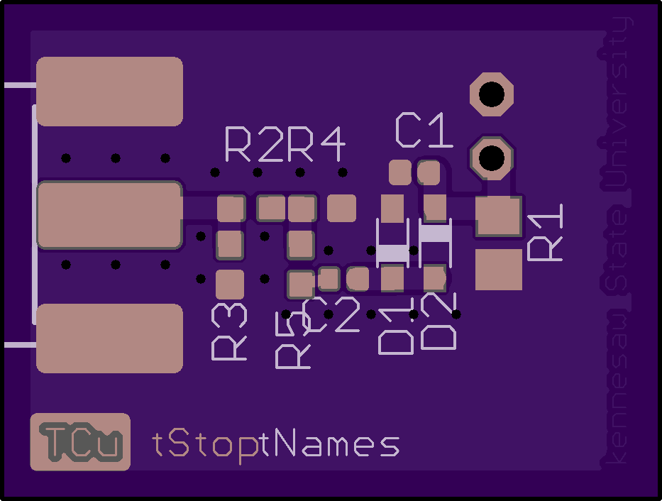

Top Bottom
Conclusion (5%)
A paragraph summarizing the simulation results, size of board, pros and cons of the device. What kind of improvements can be made in terms of design and layout for powering IoTs. Discussion of the output voltage in reference to the input voltage.
Part II Tutorials (continuing with PCB layout techniques, including schematics, conversion to board, autorouter, and part placement)
1. Best way to use the Autorouter – Autodesk EAGLE (29 minutes)
- How to set the most optimal settings for your autorouter to give you the results you expect. Carefully clean up any quirky looking traces. You’ll learn how to customize your design rules to keep yourself and your autorouter in check during your PCB layout.
https://www.youtube.com/watch?v=Ix2gKNkraDM
2. Designing your Schematic (30 minutes)
- Learn how to setup and design your schematic. Start placing parts from your free EAGLE part libraries. Use design blocks to efficiently reuse circuits from other electronics projects and save time. Verify connectivity between all of your parts with an Electrical Rule Check (ERC) on your PCB board.
https://www.youtube.com/watch?v=Jo61sGGtlKg&list=PL1rOC5j_Fyi6ZP1vBWyQFxpJ7d8T_BxoB&index=14&t=0s
3. Making a PCB Board from your Schematic (1 hr 9 min)
- Learn how to design your PCB Board from your Schematic.
- Use any one of your previous schematics from Eagle or ADS to convert to PCB following the general guidelines shown in this video.
https://www.youtube.com/watch?v=2aFNypxILu0&list=PL1rOC5j_Fyi6ZP1vBWyQFxpJ7d8T_BxoB&index=19&t=0s
Submission:
1. Report – word or pdf document with screenshots, labeled with description of the figures. (Reader should be able to understand what the figures are about.). The final schematic/board screenshots are needed for each tutorial video.
2. EagleCAD files (.sch and .brd files)
 Talk to us support@bestqualitywriters.com